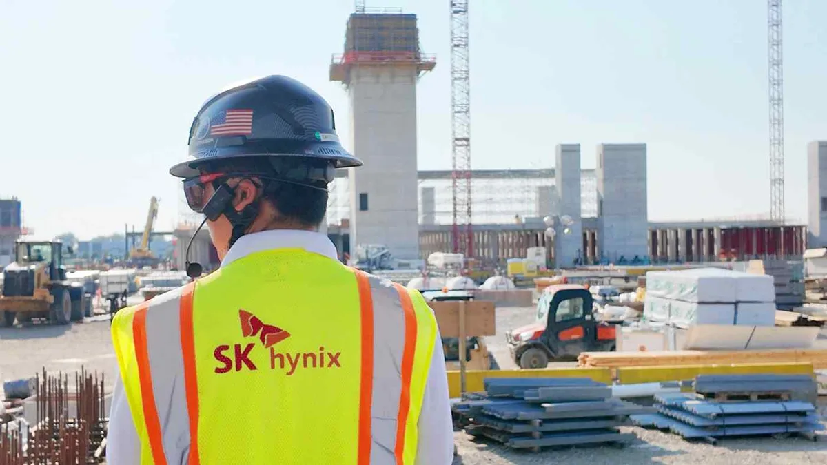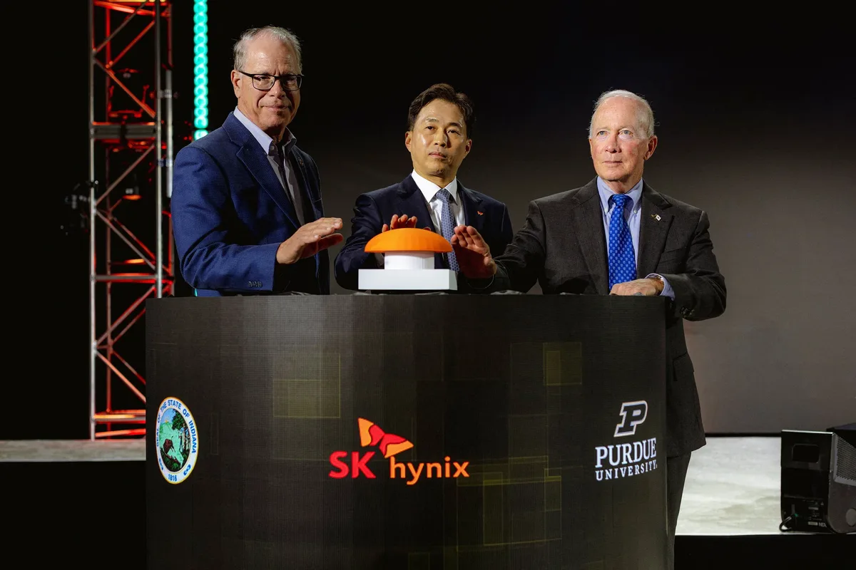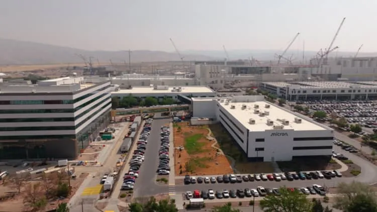
SK Hynix started formal construction on August 27, 2026, for a $4 billion memory chip packaging and AI research facility in West Lafayette, Indiana [1, 2, 3]. The plant will focus on packaging high-bandwidth memory (HBM) chips produced in South Korea and China [1, 2, 3].
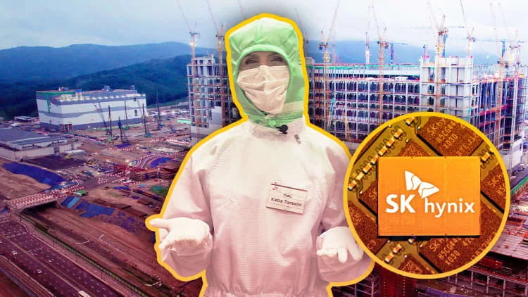
Cleanroom operations at the Indiana site are scheduled to begin in the second half of 2028, with volume production of next-generation HBM4E chips set for the third quarter of 2029 [1, 2, 3]. The company expects the facility to become a key high-bandwidth memory production base in the U.S. by 2030 [1, 2, 3]. It aims to eventually reach an annual capacity of hundreds of thousands of wafers [2, 3].
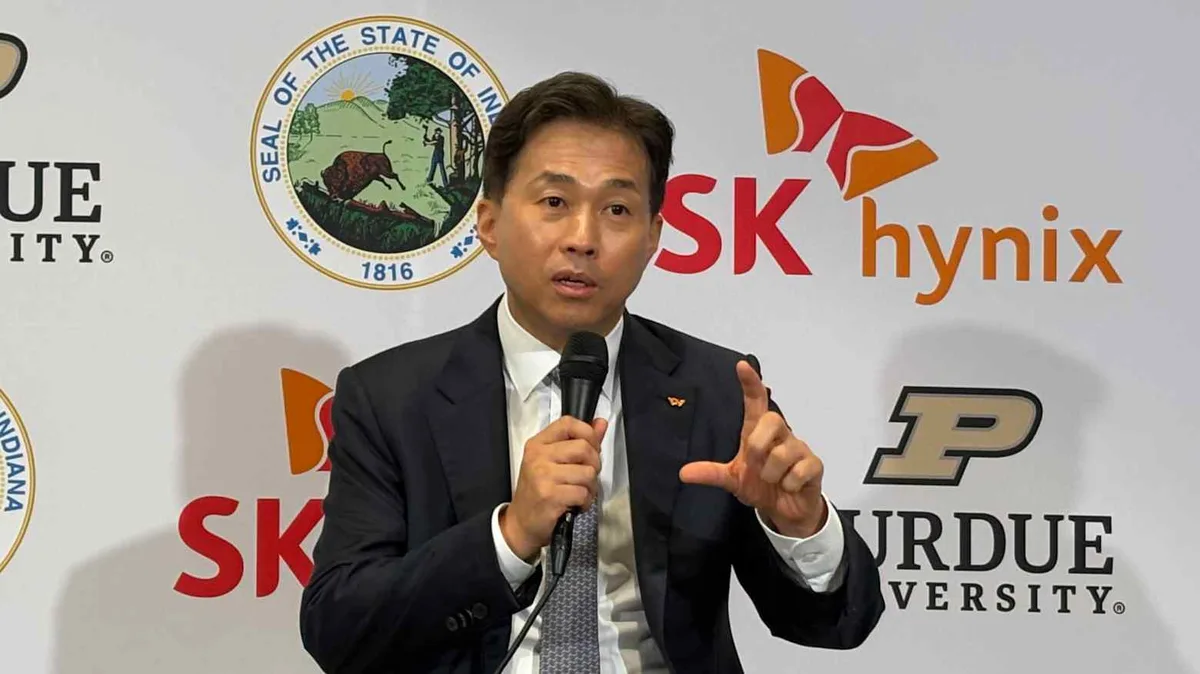
SK Hynix CEO Kwak Noh-Jung highlighted the facility's strategic importance, saying, "We will provide our customers with a new source of made-in-U.S. HBM, while strengthening the U.S. semiconductor supply chain and contributing to national and economic security" [1]. The firm noted the project connects their Korea-U.S. production system amid intensifying competition to expand AI infrastructure [2].
Kwak also said demand from AI customers remains strong and sees no signs of an oversupply risk through 2030. "I see no signal for chip oversupply risk or a potential downturn to come," he said [4]. SK Hynix expects the global memory chip shortage to last through the end of 2030 with no oversupply risk evident [4, 2, 3].
The company is spending more than $720 billion globally on memory chip production expansion, mainly in South Korea, and is open to additional U.S. investment and sites [1]. SK Hynix raised $26.5 billion in a July Nasdaq IPO and plans a possible U.S. listing for its Nand flash unit Solidigm, although no final decision has been made [1, 2, 3].
The Indiana facility marks a strategic milestone as SK Hynix aims to boost its presence in the U.S. semiconductor ecosystem. Cleanroom operation start targets range from July to December 2028, followed by production ramp-up for HBM4E chips in the third quarter of 2029 [1, 2, 3].