Intel launched the 8087 floating-point coprocessor in 1980 to boost math performance for its 8086 processor, delivering computation speeds up to 100 times faster than previous hardware [1, 2]. The chip handled arithmetic, square roots, and transcendental functions including tangent, exponentiation, and logarithms [1, 2].
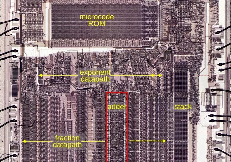
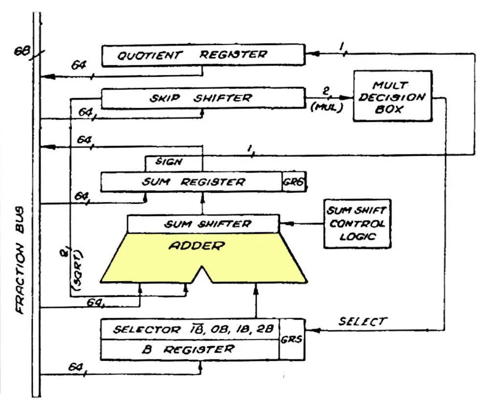
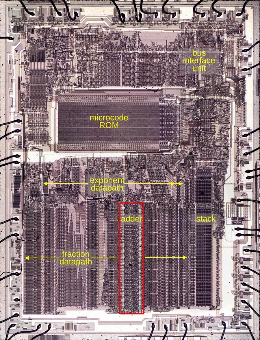
At the heart of the 8087’s floating-point unit is a 69-bit adder supported by registers, shifters, and control circuits designed to accelerate operations [1, 2]. The chip layout places a Bus Interface Unit at the top, tasked with coordinating data flow between the main 8086 processor and memory, while a large microcode ROM occupies the central area of the die [1, 2].
The bottom half of the chip - called the datapath - is split into separate exponent and fraction datapaths. The 69-bit adder itself sits in the middle of the fraction datapath, playing a critical role in speeding calculations [1, 2].
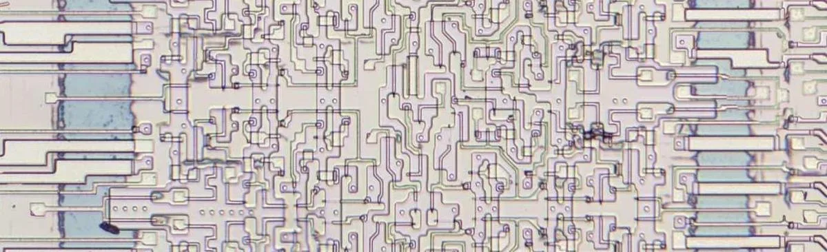
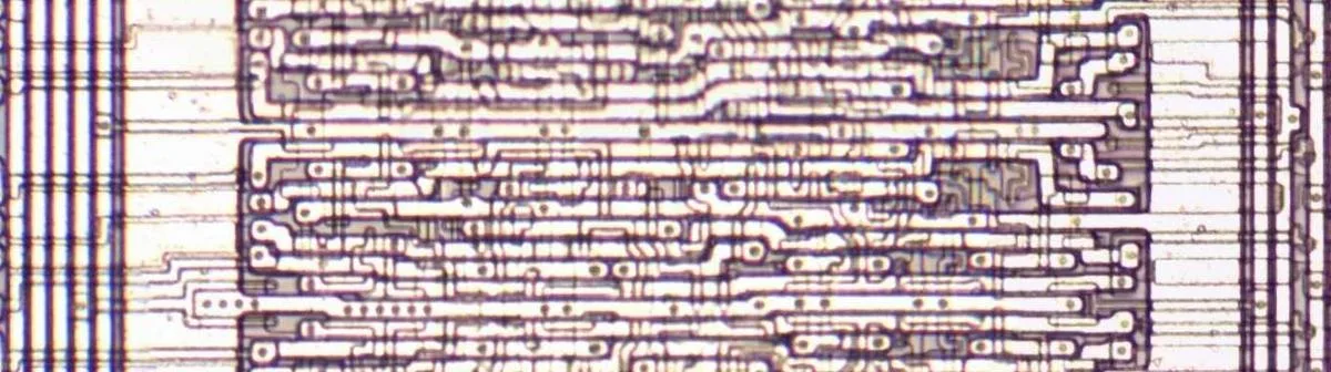
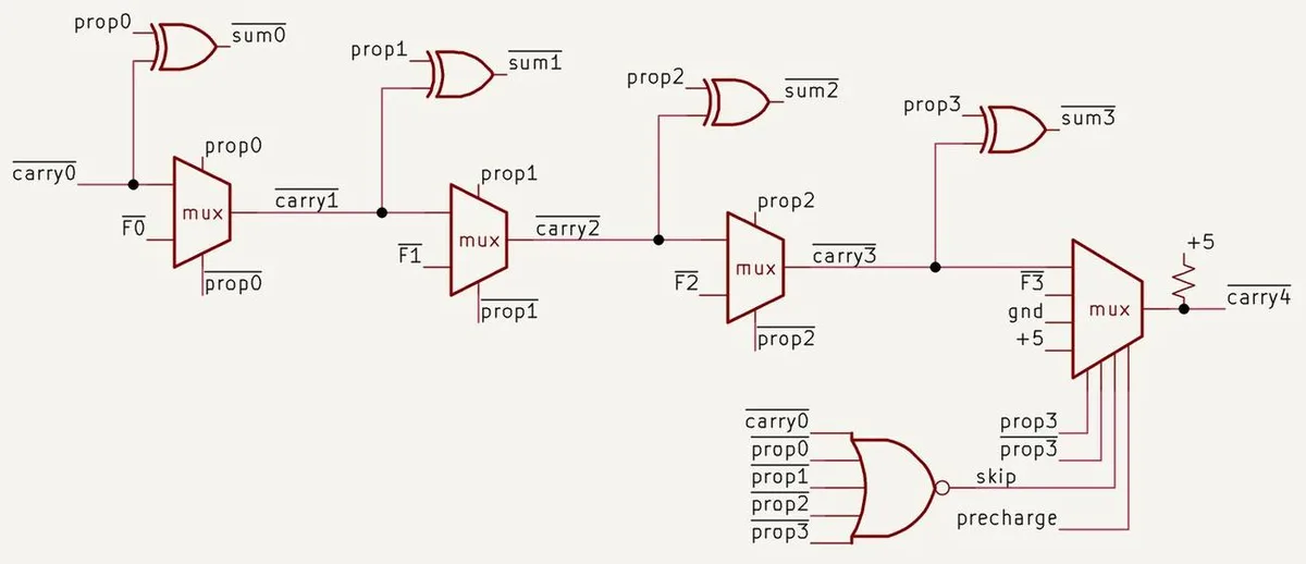
Building a fast 69-bit adder required overcoming the challenge of quickly handling carry bits, which normally must propagate through every bit sequentially and slow addition [1, 2]. Intel accelerated addition by dividing the 69 bits into 4-bit blocks and optimizing carry generation and propagation within each block, cutting the number of carry steps roughly by four [1, 2].
The adder takes two inputs: one from the fraction datapath bus and another from a register known as the B register, enabling it to perform its calculations efficiently [1, 2].
The 8087’s combination of microcode and hardware design allowed it to significantly improve floating-point math speed when paired with the Intel 8086 CPU, influencing PC computing in the early 1980s [1, 2].